Learn More about the Real Process of Electronic Assembly
NOTE: The QR codes scattered throughout the SOIC and SOT book redirect here to the section matching the phase of the assembly story. After reading the book with the child, go back to their favorite parts and call up the video to show them how that part happens in the real world!
(NEW) Full PCB Assembly Video
Manufacturing
Microchip Assembly Process: Birth of a microchip, “bunny suits” and more!
The process of creating semiconductor microchips goes far beyond the engineers who design the part, but also the production of substrates, the silicon ingots and wafers, the wafer processing machinery, and the packaging of the device itself (encapsulation) and the packaging to protect, carry and store the finished device so that it can be safely placed on circuit boards. The supporting careers for all of these steps are immense, are world wide, and everyone plays a critical role!
If one step is excluded on one component in one subsystem, no smartphones, automobiles or computers could be created.
Circuit Board Assembly Process: The real SOIC and SOT go through a Surface Mount Assembly process.
Function specific microchips are assembled on Printed Circuit Boards (PCB) to create high level systems like smartphones and computers.
Packaging
Tape and Reel Packaging
Finished microchips are stored and shipped in layers of film on reels, like classic movie films.
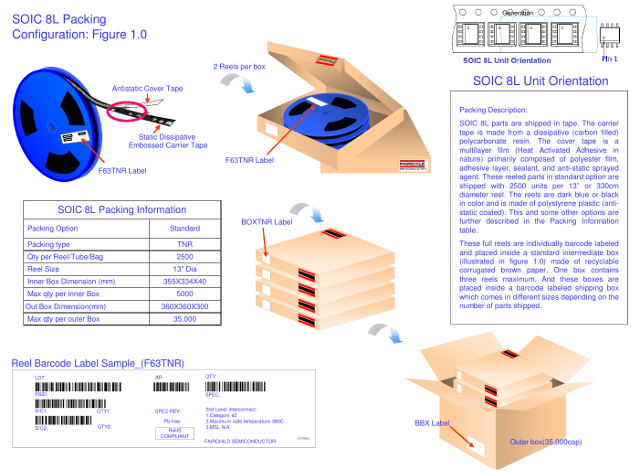
Take a look at one of millions of actual packaging specifications for one actual SOIC device here. Many marketing, sales, drawing, writing, materials specialists and management are required to make sure all of these specifications match up in the real world.
Microchip Packaging – Encapsulation
Semiconductor chips are placed on metal leadframes (legs) and then filled with plastic to form the bodies.
Placement
Pick and Place
SOIC is frightened when the Surface Mount placement machine “chunk, chunk, chunk’s” it’s way toward him. But as you’ll see in this video of a state-of-the-art “pick-and-place” machine, this fast and gentle robot carries the parts with the grace of a ballet dancer!
Also Click Here to test your skill as a pick-and-place machine!
Soldering
Infrared Reflow Process
Making all of the thousands of connections between the chips at once!
Here is a great animation of that oven, (you might recognize it correctly as an advanced industrial kitchen toaster oven) Starting at 1:25 in the video, you’ll see the actual “SOIC & SOT View” you can imagine as they are “eaten” by the big scary oven. And in the bottom left “zoom” window you can see an excellent capture of a SOIC or SOT “leg” melting the microsphere “grey goop” of solder into “warm bubbly” molten solder during the warming-cooling profile of the oven.
This is not “glue” although it looks like a paste and is called “solder paste.” It is actually millions of tiny soft metal balls, as small as dust, suspended in a gel that keeps the metal pure and clean as it melts and flows.
Testing
Inspection and Automated Test
While testing is only briefly mentioned in the book, it is a critical element of production to catch assembly errors as soon as possible. As very expensive systems are assembled, the further down the process the mistakes go, the harder and more expensive they are to correct.
After assembly, the boards are placed on a “bed of nails” tester that has “pogo pins” which touch critical test points in the circuits, and the board is quickly powered up and runs a few basic tests to see if everything is there.